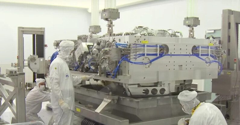
Imec, a leading semiconductor research company based in Belgium, today announced a series of chipmaking breakthroughs at its joint lab with ASML.
The lab opened its doors in June with the aim to provide ecosystem partners with early access to the High NA EUV prototype scanner.
The High NA machine represents the latest advancement in extreme ultraviolet (EUV) lithography systems, which use light to draw chip patterns on silicon wafers. It’s ASML’s most high-end tool to date.
Now, imec says that the use of the technology has already yielded impressive results.

The <3 of EU tech
The latest rumblings from the EU tech scene, a story from our wise ol’ founder Boris, and some questionable AI art. It’s free, every week, in your inbox. Sign up now!
The first is the successful printing of circuit patterns for logic chips with 9,5nm dense metal lines, which correspond to a 19nm pitch and sub-20nm tip-to-tip dimensions. This essentially translates to super small and densely-packed circuits that can deliver more powerful and efficient chips.
imec also demonstrated High NA lithography’s capability to enable 2D routing in logic chips. 2D routing refers to the process of creating intricate pathways on a single layer of a chip to connect various components or circuit elements.
In addition, the Belgian research company said it has managed to pattern designs for Dynamic Random-Access Memory (DRAM) chips in a single exposure.
Exposure is the process when light is used to transfer a pattern onto a semiconductor wafer. DRAM chips typically require multiple exposures, which means that reducing the number to one can significantly bring manufacturing costs down.
The patterns for the logic chips were also printed in a single exposure.
According to imec, these early demonstrations confirm ASML’s claims that the High NA machines can manufacture smaller, faster, and more energy-efficient chips.
“High NA EUV will therefore be highly instrumental to continue the dimensional scaling of logic and memory technologies,” said Luc Van den hove, president and CEO of imec.
Van den hove also pointed out that these demonstrations will “accelerate” the introduction of these tools into manufacturing.
Intel was reportedly the first to purchase ASML’s High NA machines in May this year. The list of buyers also includes Samsung and chip giant TSMC, although the latter was initially sceptical about the technology.
Published


